The CHK025A GaN transistor features 25W output power, 55% maximum power added efficiency (PAE) and wideband capability up to a frequency of 5GHz, compatible with both pulsed and carrier wave operation modes. With a drain to source voltage of 50V, quiescent drain current is 200mA.
The CHK040A-SOA transistor offers 40W minimum output power (50W maximum), 55% PAE, and a wideband capability up to 3.5GHz. With a drain to source voltage of 50V, quiescent drain current is quoted at 300mA.
The CHK080A device contains two identical GaN transistors to provide 80W output power, 55% PAE and a frequency range up to 3.5GHz, compatible with both pulsed and CW operation. With a drain to source voltage of 50V, quiescent drain current is 600mA, split equally across both transistors.
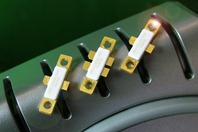
All devices in this range are supplied in a low parasitic, low thermal resistance, ceramic package with metal flange, designed for easy mounting on to a thermal heat sink, also used as main electrical ground. These components require additional external matching circuitry.
Designed and manufactured in Europe by United Monolithic Semiconductor, on a 0.5µm gate length GaN HEMT process, the transistors are RoHS and REACH compliant. For further information and advice contact Admiral Microwaves.