 In the late 90s, the top-level SPICE simulation of a 10-bit pipeline ADC design to measure signal noise and distortion (SINAD) required roughly 128 hours to complete. That same simulation in 2015 required about 10 minutes to run, with half the performance improvement due to better computer hardware and the other half due to improvements in numerical analysis engines within the SPICE simulators. The practical effect of using state-of-the-art SPICE simulators with multi-core servers was performing design verification that was previously not possible. Running a 256-iteration Monte Carlo simulation of the ADC—using a 16-core machine—means that the simulation would be complete in under three hours.
With this, one might think that all simulation problems are solved; but the story is more complicated. The same law that benefits us causes us headaches too—that is, while Moore’s law gives us significant boosts to simulation performance and capacity, it also presents significant challenges due to design size.
Emerging Simulation Challenges
One key impact of system-on-chip (SoC) design is that analog designers must design high-performance analog IP using the same processes that digital designers use. So, analog designs must now be designed without access to the precision transistors and passive elements that analog designers have relied on for past designs. As a result, designers must re-architect their circuits to take advantage of the features of deep submicron and advanced-node processes—namely, high-density logic—to implement analog functions.
However, these new architectures place divergent requirements on simulators. The only method to analyze linearity and noise in the time domain is to use transient analysis and then use Fourier analysis to convert the time domain response into the frequency domain response. This type of analysis may vary from analyzing offset voltages in comparators, to calibrating voltage-controlled oscillators in PLLs, or even designing all digital PLLs. However, there is also a need for analog functional verification because these new architectures consist of many elements that interact in many different modes of operation.
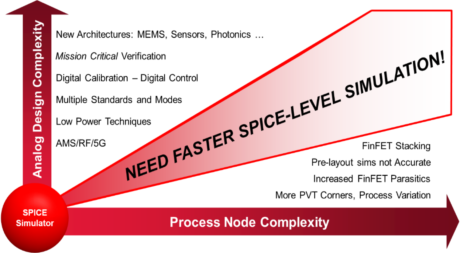 The second effect of Moore’s law is the effect of process scaling. As size has scaled down, the relative impact of the interconnect and device parasitics has increased. Traditionally, analog designers performed most of their design testing using pre-layout schematic simulation to analyze the effect of transistors on circuit performance. The recent trend has been that even the pre-layout simulations for advanced-node designs behave like post-layout simulations due the large number of devices parasitics included in the transistor models. The challenge of designing high-performance analog circuits with advanced-node transistors is compounded by the need to perform these simulations with post-layout parasitics since the ratio of transistors to parasitic RC elements can exceed 1:100.
The third effect of Moore’s law is the effect of More than Moore, which manifests itself in bigger, highly integrated designs that can require new architectures. With this effect, increased levels of integration are not achieved with increased scaling. Alternative methods are used to increase the level of integration in advanced packaging, stacking, and new materials. For example, consider new technologies, such as 3D Flash memory and magnetic memories. 3D Flash memories can store multiple bits of data in a single memory cell. Storing multiple bits in a memory cell requires sophisticated programming and read algorithms that can only be simulated using SPICE.
So we are left with a conundrum. We need traditional SPICE simulators to ensure accuracy, but we have trouble simulating the massive increases in devices and post-layout parasitics and are not able to cope with the new architectures. Traditional FastSPICE simulators could handle the new capacity needs, but their accuracy level is not acceptable to analog designers (Fig 1).
It’s time to…
The time has come, where we need to step back and re-examine the latest needs of the analog community.
It’s time to leverage modern compute hardware to perform massively distributed simulations which turn simulation days into hours.
It’s time to optimize communications between processors because SPICE simulation uses a single-time step and the coupling between the different pieces of the circuit matrix distributed across the hardware means that information needs to be shared at each time step.
It’s time to upgrade the mathematical analysis techniques to optimize device modeling and post-layout simulation that keep the golden accuracy but provide improved performance.
It’s time to allow the analog design community to fully verify their largest designs, adopting a use mode of “verification on demand” to ensure a highly tested end-product? Today’s CMOS image sensors are physically large (150K transistors), and the simulations need to include the layout parasitics (40M+ Rs and Cs).
Welcome to the new Cadence® Spectre® X Simulator, where engineers can now analyze designs that previously could only be estimated through abstractions, circuit partitioning, and extreme parasitic reductions. Just the type of technology they need as they grapple with the challenges of verifying the performance of circuits for emerging designs. Learn more: www.cadence.com/go/SpectreX
