While there are multiple methods for applying plasma to a product’s surface, one of the most popular and accessible are plasma pens.
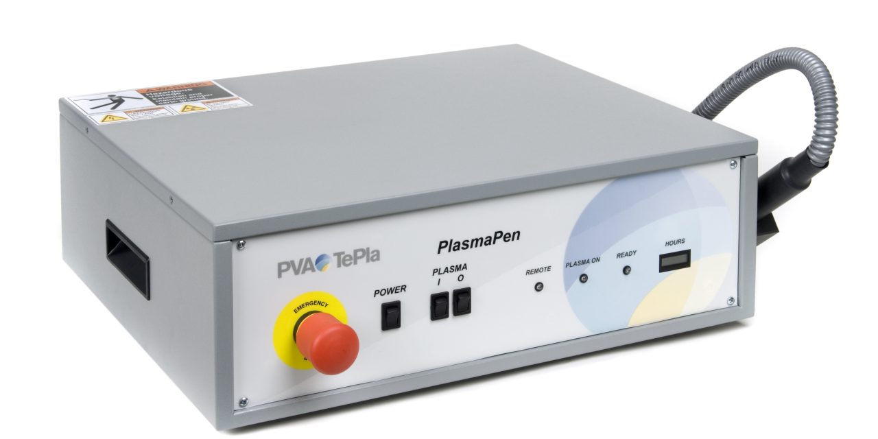
PVA TePla’s PlasmaPen is described as “a cutting-edge tool designed to enhance adhesion in electronics manufacturing”. By utilizing atmospheric plasma, the pen modifies the surface properties of printed circuit boards and electronic components, significantly improving bonding strength for adhesives, inks, coatings, and overmolding applications.
The primary advantage of the PlasmaPen is its ability to increase surface energy, making materials more receptive to bonding. This results in stronger, more reliable adhesion for critical electronic components, preventing issues such as delamination, air pockets, and moisture ingress that can lead to corrosion or electrical shorts.
A key secondary benefit is its precision in surface treatment. The PlasmaPen can be applied to targeted areas or entire components, ensuring uniform activation without compromising the underlying material. Unlike traditional surface preparation methods, it effectively cleans, roughens, or chemically modifies surfaces while remaining safe for heat-sensitive and delicate electronics.
Designed for seamless integration into automated manufacturing lines, the PlasmaPen supports customizable programming and robotic operation, allowing manufacturers to enhance their processes with minimal disruption. With options for different plasma plume sizes, cooling features, and optimized application angles, PVA TePla’s PlasmaPen provides an efficient, scalable solution for overcoming adhesion challenges in the electronics industry.
